


How does the electromagnetic compatibility (EMC) design of the OBD II connector ensure the reliability of diagnostic signals in complex automotive environments?
Release Time : 2026-02-18
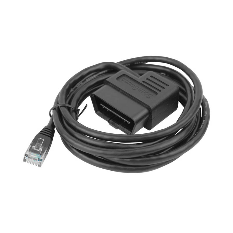
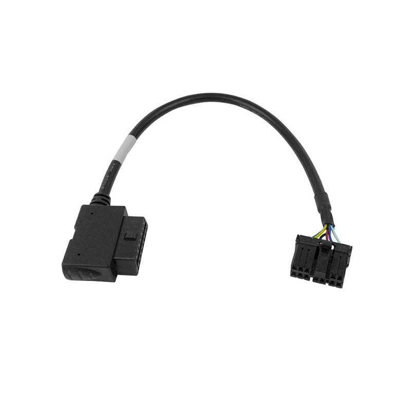
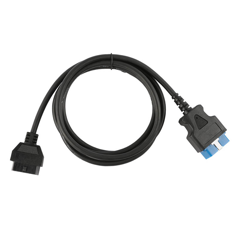
In the context of increasingly complex modern automotive electronic systems, the OBD II connector, as the standard interface between the vehicle and external diagnostic equipment, plays a crucial role in transmitting critical fault codes, real-time data streams, and control commands. However, the interior of a car is a typical environment with strong electromagnetic interference—ignition systems, motor drives, high-voltage wiring harnesses, CAN buses, etc., all generate wide-spectrum noise. If the OBD II connector lacks an effective EMC design, it can easily lead to diagnostic signal distortion, communication interruption, or even false triggering of control commands. Therefore, its structure, materials, and layout must be precisely engineered to ensure stable and reliable operation in harsh electromagnetic environments.
1. All-Metal Shielded Housing: Building the First Electromagnetic Barrier
The OBD II connector typically uses a one-piece molded metal housing that completely encloses the 16 internal signal terminals. This metal housing not only provides mechanical protection and prevents mis-mating, but more importantly, it acts as a Faraday cage, effectively shielding external radiated interference and suppressing internal signals from radiating outwards. When the connector mates with the diagnostic equipment, the metal housing forms a 360° continuous conductive contact with the diagnostic tool housing through spring contacts or conductive pads, ensuring the shielding layer is fully continuous and avoiding common-mode noise coupling caused by the "antenna effect." This fully enclosed shielding structure is the foundation for ensuring the immunity of low-speed K-line and high-speed CAN signals.
2. Low Impedance Grounding and Equipotential Connection
Good grounding is the core of EMC design. The metal housing of the OBD II connector is directly connected to the vehicle ground through a low-inductance path and maintains equipotential with the vehicle's grounding point. This not only provides a low-impedance discharge path for interference currents but also prevents electrostatic discharge caused by potential differences from damaging the internal ECU. Some high-end designs also integrate TVS diodes or common-mode chokes inside the connector to further suppress surges and high-frequency noise. Simultaneously, signal ground and power ground are strictly separated inside the connector to prevent high-current loop noise from entering sensitive diagnostic circuits.
3. Terminal Layout and Differential Signal Optimization
The OBD II standard defines the functions of 16 pins, among which CAN_H and CAN_L use differential transmission, which inherently has strong immunity to common-mode interference. To maximize this advantage, the connector's internal terminal layout follows the principle of "differential pairs adjacent, away from power/high current lines" to reduce crosstalk. Simultaneously, critical signal lines utilize shorter traces and impedance matching designs to reduce reflections and ringing. The plastic insulator is made of engineering plastic with low dielectric constant and low loss factor to minimize signal attenuation. Furthermore, unused pins are typically left floating or grounded to avoid becoming antenna noise.
4. Automotive-grade materials and processes ensure long-term reliability
OBD II connectors must meet automotive-grade standards such as AEC-Q200, maintaining stable performance under temperature cycling from -40°C to +125°C, high humidity, salt spray, and vibration environments. Terminal surfaces are generally gold-plated or tin-plated: the gold layer provides ultra-low contact resistance and excellent oxidation resistance, ensuring that weak diagnostic signals are not distorted; the tin layer balances cost and solderability. The shell plating combines conductivity and corrosion resistance, maintaining shielding effectiveness even in humid or sulfur-containing environments. Strict injection molding process control ensures the insulator is free of bubbles and internal stress, preventing cracking and shielding failure during long-term use.
Despite its small size, the OBD II connector is a model of electromagnetic compatibility design in automotive electronic systems. Through the synergy of metal shielding, scientific grounding, signal optimization, and automotive-grade materials, it successfully constructs a "clean" diagnostic data channel in the electromagnetically noisy automotive environment. This reliability not only ensures maintenance efficiency and driving safety but also lays a solid physical foundation for future connected vehicles, remote upgrades, and intelligent diagnostics. In the era of software-defined vehicles, a small 16-pin interface remains a crucial bridge connecting the digital world and the steel body.